
 Ultra-Flat Thermal 6" SiO2 Wafer 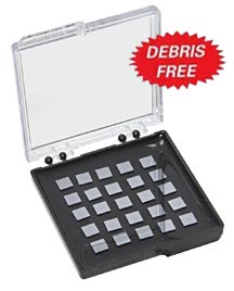 5 x 5mm Diced Ultra-flat Thermal SiO2 Substrates |
Ultra-Flat Thermal SiO2 SubstratesThe Ultra-Flat SiO2 substrates consist of a 200nm thermally grown amorphous SiO2 film on an ultra-flat silicon wafer. SiO2 is one of the most characterized materials and is widely used in semiconductor manufacturing, thin film research and as substrate for growing cells. It can be directly used as substrate for AFM and SEM imaging. The ultra-flat thermal silicon dioxide substrates are available in 6" wafer and conveniently diced 5 x 5mm, 5 x 7mm and 10 x 10mm chips. The 6" wafer is shipped in a 6" wafer carrier, the diced pieces are shipped in a Gel-Pak® box. The special clean dicing process involves coating the wafer with photo resist before dicing and removing it after dicing which produces debris-free SiO2 substrates. All products are packed in class 10 clean room conditions. Properties for thermal SiO2 substrates:
|
|||||||||||||||
|
||||||||||||||||
产品中心
产品详情
简单介绍:
200nm Thermal Oxide on ø6" Ultra-Flat Wafer, Type <100>, in 6" wafer carrier
详情介绍: